Tekbox TBMDA-CDN25
Tekbox TBMDA-CDN25
| Lieske Part No. | 1156164 |
|---|---|
| Mfg Part No | TBMDA-CDN25 |
| EAN-Code | |
| Manufacturer | Tekbox |
| Here only | 2.530,31 EUR
3.011,07 EUR incl. VAT
|
Further information for Tekbox TBMDA-CDN25
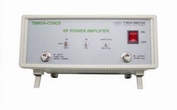
TBMDA-CDN25 Wideband Modulated Power Amplifier
The TBMDA-CDN25 modulated amplifier provides the required power, bandwidth and modulation for conducted immunity tests with CDNs and BCI probes in the frequency range 100 kHz to 250 MHz. It is designed to be driven by signal generators or tracking generators of spectrum analyzers. With a 1 dB compression point of up to 25 W in the frequency range 100 kHz to 250 MHz, it can generate test levels of classes 1, 2, 3 and X according to ISO/EN 61000-4-6. A built-in AM/PM modulator allows the use of tracking generators as a signal source. The TBMDA-CDN25 has sufficient gain to reach the maximum output power of 0 dBm provided by a spectrum analyzer tracking generator.
In addition to 1 kHz, 80% AM, the TBMDA-CDN25 offers a built-in modulation capability to generate 1 kHz, 50% duty cycle PM signals. In PM mode, the TBMDA-CDN25 can also generate a 217 Hz signal with 12.5% duty cycle to simulate the TDMA noise of a mobile phone.
FEATURESCW Amplifier (modulation off) 1 kHz, 80% AM modulation 1 kHz, 50% duty cycle pulse modulation 217 Hz, 12.5% duty cycle pulse modulation SPECIFICATIONS
Input / Output: 50 Ohm, N-female
Supply voltage range: 110 V...240 V
Supply power consumption: 108 W @ 220V
Operating temperature range: -20°C to 50°C
Frequency range: 100 kHz - 250 MHz
Small signal gain: 47 dB typ.
Gain flatness 100 kHz - 250 MHz / Pin = -3 dBm: 3.5 dB typ.
Saturated output power at 100 kHz / Pin = 0 dBm: 44.1 dBm (25.7 W) typ.
Saturated output power at 150 kHz / Pin = 0 dBm: 44.6 dBm (28.8 W) typ.
Saturated output power at 500 kHz / Pin = 0 dBm: 45.1 dBm (32.4 W) typ.
Saturated output power at 1 MHz / Pin = 0 dBm: 45.3 dBm (33.9 W) typ.
Saturated output power at 10 MHz / Pin = 0 dBm: 45.3 dBm (33.9 W) typ.
Saturated output power at 50 MHz / Pin = 0 dBm: 45.6 dBm (36.3 W) typ.
Saturated output power at 80 MHz / Pin = 0 dBm: 46.6 dBm (45.7 W) typ.
Saturated output power at 100 MHz / Pin = 0 dBm: 46.5 dBm (44.7 W) typ.
Saturated output power at 150 MHz / Pin = 0 dBm: 44.5 dBm (28.2 W) typ.
Saturated output power at 200 MHz / Pin = 0 dBm: 43.8 dBm (24 W) typ.
Saturated output power at 230 MHz / Pin = 0 dBm: 44.9 dBm (30.9 W) typ.
Saturated output power at 250 MHz / Pin = 0 dBm: 44.8 dBm (30.2 W) typ.
1dB Output compression point @ 100 kHz: +43.7 dBm typ. (Pin: -5 dBm)
1dB Output compression point @ 150 kHz: +44.1 dBm typ. (Pin: -4 dBm)
1dB Output compression point @ 500 kHz: +44.6 dBm typ. (Pin: -3 dBm)
1dB Output compression point @ 1 MHz: +45 dBm typ. (Pin: -3 dBm)
1dB Output compression point @ 10 MHz: +45 dBm typ. (Pin: -2 dBm)
1dB Output compression point @ 50 MHz: +45.6 dBm typ. (Pin: 1 dBm)
1dB Output compression point at 80 MHz: +46.5 dBm typ. (Pin: 1 dBm)
1dB Output compression point at 100 MHz: +46.5 dBm typ. (Pin: 0 dBm)
1dB Output compression point at 150 MHz: +42.9 dBm typ. (Pin: -4 dBm)
1dB Output compression point at 200 MHz: +42.2 dBm typ. (Pin: -4 dBm)
1dB Output compression point at 230 MHz: +44.1 dBm typ. (Pin: -3 dBm)
1dB Output compression point at 250 MHz: +43 dBm typ. (Pin: -4 dBm)
2nd harmonic, 100 MHz, Pout=46dBm: < - 12 dBc typ. 2nd
harmonic, 100 MHz, Pout=40dBm: < - 15 dBc typ.
3rd harmonic, 100 MHz, Pout=46dBm: < - 22 dBc typ.
3rd harmonic, 100 MHz, Pout=40dBm: < - 22 dBc typ.
Total harmonic distortion
17.7% @100MHz, Pout=37dBm typ.
19.6% at 100 MHz, Pout=40 dBm typ.
22.1% at 100 MHz, Pout=43 dBm typ.
26.9% at 100 MHz, Pout=46 dBm typ.
Third order output intercept point: +51 dBm, @100 MHz, ? f = 2MHz, typ.
Internal modulation frequency AM: 1 kHz ±20%
Internal modulation frequencies PM: 1 kHz ±20%, 217 Hz ±20%
Duty cycle, PM: 50% ±10% at 1 kHz 12.5% ±20% at 217 Hz
Maximum ratings
Maximum input power: +3 dBm
The output of the TBMDA-CDN25 is quite tolerant of output mismatches, however an open or short circuited load is not recommended as this may potentially cause damage to the output transistor. When operating near field probes, current probes or other loads with unknown impedance, it is strongly recommended to insert an attenuator of = 3dB at the output of the amplifier to protect the output stage.
Application
General purpose wideband RF power amplifier
Wideband RF power amplifier for conducted immunity testing with CDNs or BCI probes
Broadband RF power amplifier for radiated immunity testing, driving near-field probes
Broadband RF power amplifier for radiated immunity testing, driving TEM cells

This is an offer of:
79279 Vörstetten
https://industry-electronics.com
Tel. 07666/88499-0
Fax. 07666/88499-111
Diesen Artikel finden Sie unter:
industry-electronics.com/artikel/1156164

Lieske Elektronik e.K.
Reutener Str. 1079279 Vörstetten
https://industry-electronics.com
Tel. 07666/88499-0
Fax. 07666/88499-111
Diesen Artikel finden Sie unter:
industry-electronics.com/artikel/1156164